A (very) close look at the A17 Pro chip powering the iPhone 15 Pro
-
by Anoop Singh
- 12

The A17 Pro chip powering the iPhone 15 Pro and Pro Max models was the first in the world to use a 3-nanometer process, and Apple is already looking ahead to a 2nm chip in 2025, and a 1.4nm one beyond that, perhaps as early as 2026.
A new report today takes a fascinating look at just what is involved in these unimaginably small process sizes …
A17 Pro chip
Apple said that the A17 Pro chip included its biggest ever leap in GPU design.
iPhone 15 Pro and iPhone 15 Pro Max are powered by A17 Pro, the industry’s first 3-nanometer chip. Continuing Apple’s leadership in smartphone silicon, A17 Pro brings improvements to the entire chip, including the biggest GPU redesign in Apple’s history.
The new CPU is up to 10 percent faster with microarchitectural and design improvements, and the Neural Engine is now up to 2x faster, powering features like autocorrect and Personal Voice in iOS 17.
The pro-class GPU is up to 20 percent faster and unlocks entirely new experiences, featuring a new 6-core design that increases peak performance and energy efficiency. Now with hardware-accelerated ray tracing — which is 4x faster than software-based ray tracing — iPhone 15 Pro offers smoother graphics, as well as more immersive AR applications and gaming experiences. iPhone 15 Pro brings true-to-life gaming to the palm of users’ hands with console titles never before seen on a smartphone.
Unimaginable scale
While the nanometer numbers once referred to the physical size of transistor gates, that’s no longer the case. Instead, the numbers aim to provide a basis for understanding the shrinking scale of the components.
The Financial Times focus on the chip design notes that the transistors used are now built atom-by-atom, and turn on and off billions of times per second.
Just one square millimetre can be home to 200 million transistors, with tens of billions across a chip. Manufacturers plan to cram in a trillion in the not-too-distant future.
Another way to think about the scale is that the transistors are joined together using metal wire. How much wire is squeezed into these chips? Almost 500km (310 miles)!
Reflected in the fabrication costs
TSMC leads the world in ever smaller chip processes, which is why it is the sole supplier of Apple’s A-series and M-series chips: No other chipmaker is capable of working at these tiny sizes.
But the complexity of the task is reflected in the costs of designing and building these chips. In the shift from 10nm to 5nm, for example, it’s estimated that the cost to Apple of designing a new chip increased from $174M to $540M. The cost to TSMC of building a fabrication plant for these chips rose from $1.7B to $5.4B in the same time.
Reaching the limits of physics
The overall process of making a chip from sand hasn’t changed much. We still heat up sand, extract the silicon, use a rod to create a wine-bottle-shaped ‘boule,’ slice that into wafers, polish these, etch patterns into them, blast ions at them to create conductive and insulating areas, and add wires to connect the transistors.
What has changed is complexity and precision of the etching and wiring stages.
For the smallest chips, multi-million-dollar machines made by a single Dutch company, ASML, use extreme ultraviolet light to create these fine stencils. The machines are the size of a bus, but so accurate they could direct a laser to hit a golf ball as far away as the Moon.
We’re now approaching the limits of physics in terms of how much smaller the process can get, which is why the latest chip designs stack multiple layers together.
“You’re really starting to expand that third dimension, which is something that hasn’t been used in the first 60 years of transistor technology,” says Intel’s Auth. “[When] you build skyscrapers, you start to run out of the ability to shrink things laterally, so you start to build up and that’s what we’re doing” […]
This pivot to vertical design and development is “kind of a big deal”, says Koch of SemiAnalysis, because it is the first time the industry has acknowledged that it’s running out of horizontal options. “We’re slowing down in one direction, but speeding up in another,” he says.
Apple’s approach of packaging together different chips – or ‘chiplets’ – is also seen as the future.
Packaging developments have paved the way for another shift in semiconductor architecture: “chiplets”.
Engineers are moving away from building an entire microprocessor on a single piece of silicon — the monolithic “system on a chip” — and towards multi-chip modules (MCMs). These MCMs see groups of chips with different functions built on separate pieces of silicon and then bundled together to work like a single electronic brain.
Another planned development is to separate power and signal wiring – something that has never been done before.
Power wires will move from the top (front), to the bottom (back side) of the chip, sitting below the transistor layer, rather than above. The interconnects will stay put. Early tests show this direct route for power and reduced tangle of wires results in greater efficiency.
The whole piece is well worth reading.
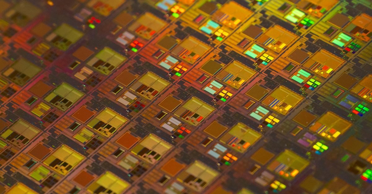
Photo by Maxence Pira on Unsplash
FTC: We use income earning auto affiliate links. More.
The A17 Pro chip powering the iPhone 15 Pro and Pro Max models was the first in the world to use a 3-nanometer process, and Apple is already looking ahead to a 2nm chip in 2025, and a 1.4nm one beyond that, perhaps as early as 2026. A new report today takes a fascinating look…
The A17 Pro chip powering the iPhone 15 Pro and Pro Max models was the first in the world to use a 3-nanometer process, and Apple is already looking ahead to a 2nm chip in 2025, and a 1.4nm one beyond that, perhaps as early as 2026. A new report today takes a fascinating look…
